|
|
|
|
|
|
|
|
|
 |
HOME > Introduction > Research Field |
|
|
1. Heterointerface 2DEG Transparent and Foldable Functional Materials and Devices 
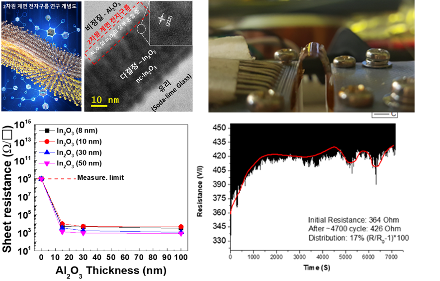
Traditional transparent oxide semiconductors (TOSs), such as Sn-In2O3 (ITO) are facing up the limitation of flexibility and foldability. However, tremendous researches to improve the mobility and stability of oxide semiconductors are being continued for the successful integration of oxides to transparent and flexible electronic devices (TFT, Diodes). We suggest the heterointerfacial 2DEG transparent and foldable functional materials and devices based on atomic layer deposition (ALD). Our target oxides under study are In2O3, ZnO, IGZO, ITO and CuO, NiO, SnO for the n-type TOSs and for the p-type TOSs, respectively. The ultimate-goal is to achieve the ultra-flexible transparent logic device and transparent electrode using interfacial 2DEG channel. - Further Readings
- “Permanent Optical Doping of Amorphous Metal Oxide Semiconductors by Deep Ultraviolet Irradiation at Room Temperature”, Appl. Phys. Lett. 96, 222101-1~3 (2010) "A study on H2 plasma treatment effect on a-IGZO thin film transistor”, J. Mat. Res. 27(17), 2318-2325 (2012). "Dual active layer a-IGZO TFT via homogeneous conductive layer formation by photochemical H-doping”, Nanoscale Res. Lett 9:619 (2014). “Photochemical Hydrogen Doping Induced Embedded Two-Dimensional Metallic Channel Formation in InGaZnO at Room Temperature”, ACS Nano 9, 10, 9964-9973 (2015) "Creation of a Short-Range Ordered Two-Dimensional Electron Gas Channel in Al2O3/In2O3 Interfaces" ACS Nano, 11, 6, 6040-6047 (2017)
2. 2D Semiconductor and Devices 
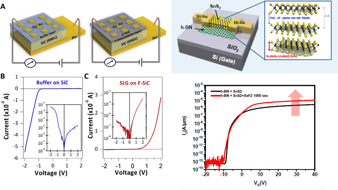
As for channel materials in next generation transistors, two-dimensional (2D) materials such as graphene and chalcogenide are potentially considered. Especially, 2D oxides are highlighted as materials class free of toxicity that chalcogenides have. We are investigating the synthesis and characterization of 2D oxides, chalcogenide nanosheets and single layer graphene semiconductor and their diodes/TFTs by functionalization with finely tuned gas-phase and low-energy ion doping technology. - Further Readings
- “Generation of Highly n-Type Titanium Oxide Using Plasma Fluorine Insertion”, Nano Lett. 11, 751-756 (2011) "Tuning the Electronic Structure of Tin Sulfides Grown by Atomic Layer Deposition”, ACS Appl. Mat & Int. 5(18), 8889-8896 (2013) “Mulit-resistive Reduced Graphene Oxide Diode with Reversible Surface Electrochemical Reaction induced Carrier Control”, Sci. Rep. 4:5642 (2014) “Visible Photocurrent in Chemically Doped TiO2-Based Schottky Diodes”, J. Am. Ceram. Soc. 98[8], 2470-2475. (2015) “Complementary Schottky diode formation with carbon buffer and p-doped single layer graphene on intrinsic SiC via fluorine intercalation”, Carbon, 142, 254-260 (2019)
3. Next Generation IC Devices: High k Gate stack, Neuromorphic Synapse Memory and Mott material-Si heterojunction hybrid FET 
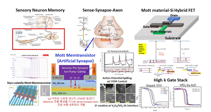
As the scaled-down integration of IC chips has been being continued, the limitations of MOSFET have been known, and the power consumption of electronic devices is increasing rapidly. Therefore, it is necessary to reduce the driving voltage in order to solve the power density issue of the IC chips with increase of the integration. At the same time, in order to maintain high driving current (ION) and low leakage current (IOFF), the subthreshold swing (SS) must be reduced.
As an alternation for MOSFETs, tunneling field effect transistors (TFET) with similar structures and processes have attracted attention. Unlike MOSFETs, TFETs can overcome the Boltzmann limit of subthreshold swing at 60 mV/dec through rapid carrier injection at low leakage current and operating conditions, resulting in super-steep switching characteristics and reliable operation.
Furthermore, we are in the process of introducing Mott material as a source to solve the low ON current, a disadvantage of TFETs. This Mott transition can be applied to next generation low power semiconductor devices through fast switching speeds (Moreover, in view of the same problem of MOSFETs, attention has been paid to neuromorphic devices optimized for parallel signal process operation. We expressed STDP through oxygen ion control using disordered VOx and we are developing a Mott “memtransistor” that can mimic to human neural network. As the dimension of IC devices is continuously scaled down, the physical limitation of materials used in the conventional IC device is apparent. This renders challenging tasks for characterization on band electronic properties of intrinsic materials and heterointerface at the ultrathin scale. We are currently developing the analytic method for ultrathin interfacial band electronic structure of dynamic random-access memory (DRAM) using XPS, UPS and Internal photoemission spectroscopy (IPS) in a combination with various electrical device analysis such as IV, CV, TDDB, BTI, SILC, Tunneling Analysis. - Further Readings
- "Reversible Bistability of Conductance on Single Layer Graphene/CuOx/Cu nanojunction”, Appl. Phys. Lett. 100, 123101 (2012) "Reversible Oxidation States of Single Layer Graphene Tuned by Electrostatic Potential”, Suf. Sci. 612, 37-41 (2013) “Resistive switching of a TaOx/TaON double layer via ionic control of carrier tunneling”,Appl. Phys. Lett. 104, 151603 (2014) "Detection of oxygen ion drift in Pt/Al2O3/TiO2/Pt RRAM using interface-free single-layer graphene electrodes”, Carbon, 75, 209-216 (2014) "Stabilzed resistive switching behaviors of a Pt/TaOx/TiN RRAM under different oxygen contents”, Phys. Status Solidi A. 211, 9, 2189-2194 (2014) “Spatially confined electric field effect for improved resistive switching behavior of a Ni/Ta-embedded TaOx/NiSi device”, RSC Adv. 4, 61064-61067 (2014) "Depth resolved band alignments of ultrathin TiN/ZrO2 and TiN/ZrO2-Al2O3-ZrO2 dynamic random access memory capacitors”, Appl. Phys. Lett. 105, 201603 (2014) "Resistive switching behaviors of Cu/TaOx/TiN device with combined oxygen vacancy/copper conductive filaments", Current. Appl. Phys. 15, 1005-1009 (2015) "Effects of the radio-frequency sputtering power of an MgO tunneling barrier on the tunneling magneto-resistance ratio for Co2Fe6B2/MgO-based perpendicular-magnetic tunnel junctions” , J. Mater. Chem. C, 4, 135-141 (2015) "Forming-less and Non-Volatile Resistive Switching in WOX by Oxygen Vacancy Control at Interfaces" Scientific Reports 7 10186 (2017) "Electric Field-Triggered Metal-Insulator Transition Resistive Switching of Bilayered Multiphasic VOX" Electron. Mater. Lett. 14 14-22 (2018)
|
|
|
|
|
 |
우443-749 경기도 수원시 영통구 원천동 산 5번지 아주대학교
Copyright(c) 2013 Advanced Electronic & Energy Materials Laboratory, All Rights Reserved. |
|
|
|